IBM Reveals Worlds First 5nm Chip
Samuel Wan / 8 years ago

Every year, the death of silicon chips draws closer, with more and more warnings. Despite that, semiconductor foundries continue to push the limits of what is possible. In the past, Intel has largely kept the lead in process nodes but this advantage is slipping away. IBM, in partnership with Samsung and GlobalFoundries, has revealed their latest 5nm silicon chips. This is the first time the public has seen a 5nm chip.

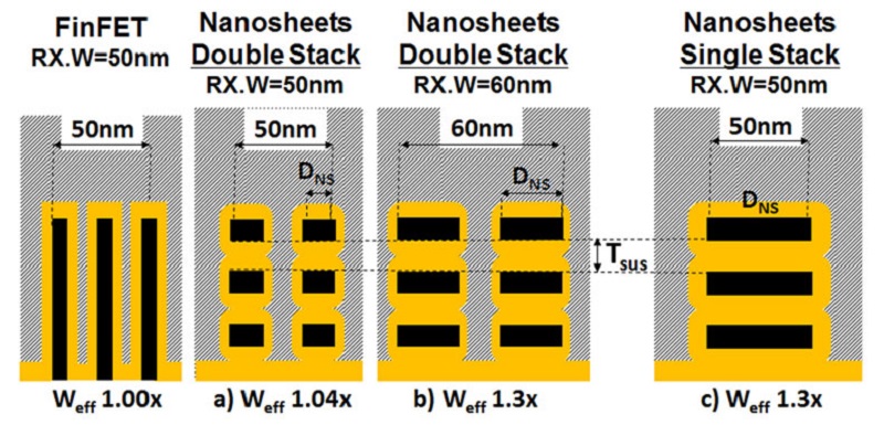
In order to reach 5nm, IBM has to resort to a whole host of new technologies. The chief advancements are the use of new finFETs and EUV. Basic finFETs are a 3D fin gate that controls the flow of electrons in the channel. While useful compared to a plain transistor, they will likely run out of steam at 7nm. To hit 5nm, IBM used their new Gate All Around or GAAFETs. Instead of having the gate warp around the channel fin, the gate now surrounds the tubular channel completely. Due to the use of GAAFETs, IBM is able to get the 5nm process to be 40% faster or use 75% less power than 10nm. Compared to 7nm, it is 50% as dense as well.

In order to get GAAFETs and 5nm to work well, IBM is also using EUV or extreme ultraviolet lithography. EUV has been touted as the next big development in lithography but has never reached the production line. It looks like IBM has managed to get EUV to work well enough for them to handle 5nm production. Hopefully, these advancements can postpone the end of silicon chips and keep chip prices low for least a few more years.


