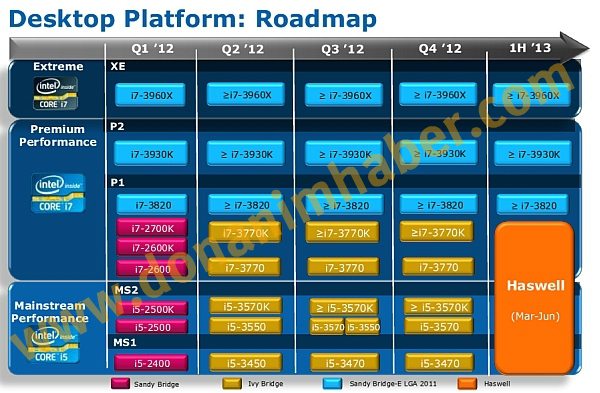
Intel’s Haswell due March 2013
Ryan Martin / 13 years ago

Intel’s program for processor development is know by the ‘tick-tock’ development. The tick is the first transition into the new process size for example the tick of 32nm was socket 1156 Nehalem. Whilst the tock is the refinement of that particular process often by redesigning the architecture so continuing to use 32nm as the example the tock of that was Sandy Bridge socket 1155. So in continuance with Intel’s tick-tock development model we know that Ivy Bridge will be the tick or Intel’s first venture into 22nm processor development and as most people know this is due some time in March/April this year. Intel’s 22nm Ivy Bridge venture will essentially be Sandy Bridge but with a miniaturization of the manufacturing process allowing for more transistors, less power consumption and greater overclocking headroom. As well as that Intel also plan to drastically redesign the IGP of the Ivy Bridge CPUs to introduce the HD 4000 series graphics which will be Direct X 11 ready and support 4K resolutions.
The tock of Intel’s development process is going to be Haswell. Essentially a refinement of the existing 22nm process introduced in the form of Ivy Bridge but with a radically new processor architecture which in theory should bring a substantial amount of performance gains alongside some efficiency gains in the form of power consumption. Earlier reports have indicated that Haswell Core processors will be based on a newer socket, the LGA1150, and hence it will not be compatible with LGA1155 platforms.
Source: DonanimHaber


