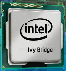
The Intel Developer Forum (IDF) conference of 2011 brought out much information to the public about the upcoming Ivy Bridge release. There was a lot of information released but we take a brief look through and summarise what is new about the world’s first consumer 22nm processors.
Firstly, there is a whole bunch of new chipset configurations as you might expect: Z77, Z75, H77, Q77, Q75 and B75 will be the full range of the new chipsets. The new features for these chipsets are:
- native PCI-E 3.0
- native USB 3.0
- Integrated graphics support among all chipset variations unlike Sandy Bridge
- High probability of smart response support on all chipsets too although the final decision on this is yet to be made.
Secondly, power consumption savings are brought about by the improved efficiency of the 22nm manufacturing process and the fact Intel brings a TDP controller with some of its Ivy Bridge CPUs which allow you to pick between a low TDP, nominal TDP or high TDP depending on whether you want maximum performance or maximum energy efficiency, ULV parts will include quad cores at just 35W.
The new re designed GPU makes use of newer graphics architecture and brings native Direct X 11 support. The Ivy Bridge graphics units also have more cores in them, 16 cores as opposed to 12 and according to Intel the number of gigaFLOPS the new graphics units can execute is much higher than Sandy Bridge and ultimately this will bring up to 66% more performance in the graphics department.
And finally the processor cores will have around 4-6% more clock for clock performance than Sandy Bridge and up to 10% when you take into consideration the higher clock speeds the smaller architecture will be able to achieve, all at the same price points.


