JEDEC Considers Wide I/O, Wide I/O 2 Interfaces for PCs and Servers.
Peter Donnell / 12 years ago

JEDEC and manufacturers of dynamic random access memory (DRAM) and memory controllers are considering to develop Wide I/O and Wide I/O 2 specifications for very high-bandwidth stacked memory devices aimed at personal computers and servers. Essentially, JEDEC is developing a rival for proprietary hybrid memory cube memory technology.
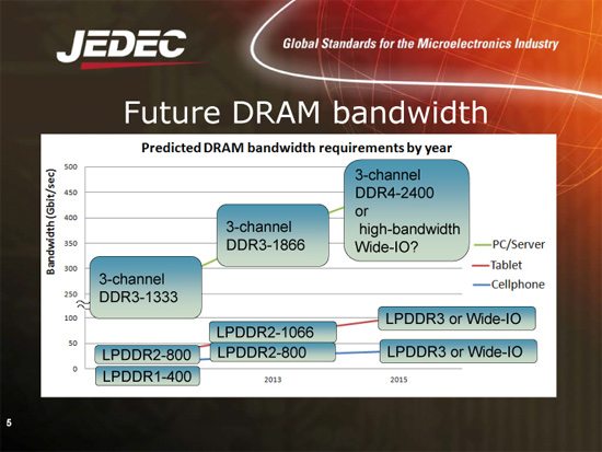
Multi-channel memory sub-systems have satisfied the needs for high memory bandwidth for over a decade now, but the recent progress with stacked chips and wide input/output (I/O) sub-systems offer to reduce power consumption of memory chips while considerably increasing their bandwidth, which means very speedy yet low power memory sub-systems. Intel Corp., Micron Technology and Samsung Electronics are already working on hybrid memory cube (HMC) technology that utilizes several DDR3 memory components stacked on each other and connected using through silicon vias (TSVs) along with wide memory bus to provides 1Tb/s (125GB/s) bandwidth from a single memory device. JEDEC is working on something similar with its wide I/O spec, according to Mobile Forum 2012 proceedings presentation, which was partly published by PC Watch web-site.

At present the wide I/O specification is designed for mobile devices. For example, Samsung Electronics demonstrated earlier this year a 1Gb DRAM chip with 512-bit bus and 12.5GB/s bandwidth. The chip corresponds to JESD229 standard and employs four 256Mb 128/-bit SDR memory components operating at 200MHz.
Possible future standards currently under consideration include 512-bit memory solutions with four 128-bit memory components operating at 533MHz effective clock-rate for mobile applications (to provide 266Gb/s or 33.2GB/s bandwidth) as well as with 2133MHz effective clock-speed for non-mobile applications (to reach 1Tb/s or 125GB/s bandwidth). The latter is a direct competitor for the HMC technology. However, JEDEC has no plans to stop there and intends to create stacked memory devices with 2Tb/s (250GB/s) bandwidth for performance-demanding applications.

At present it is unclear whether the 2Tb/s Wide-IO DRAM devices will continue to use 512-bit memory bus or will adopt 1024-bit memory bus, which is extremely hard and expensive to implement. A natural way is to continue using four components per memory device, but to migrate to 4Gb/8Gb LPDDR4 components with increased capacity and clock-speed sometimes in 2014 – 2015.

While neither the HMC nor the wide I/O technologies are free of caveats, the trend towards multi-stacked memory devices with wide memory busses is generally clear. Such devices – given that they cannot provide truly high memory capacities – will likely be used in various notebooks, ultrabooks, micro-servers, storage servers and other devices of the kind that benefit from high-speeds, but do not need extreme memory capacities.
Source: Xbitlabs


