New JEDEC Standard Allows for up to 24GB per-Stack HBM2
Ron Perillo / 6 years ago

Higher-Capacity High-Bandwidth Memory (HBM2)
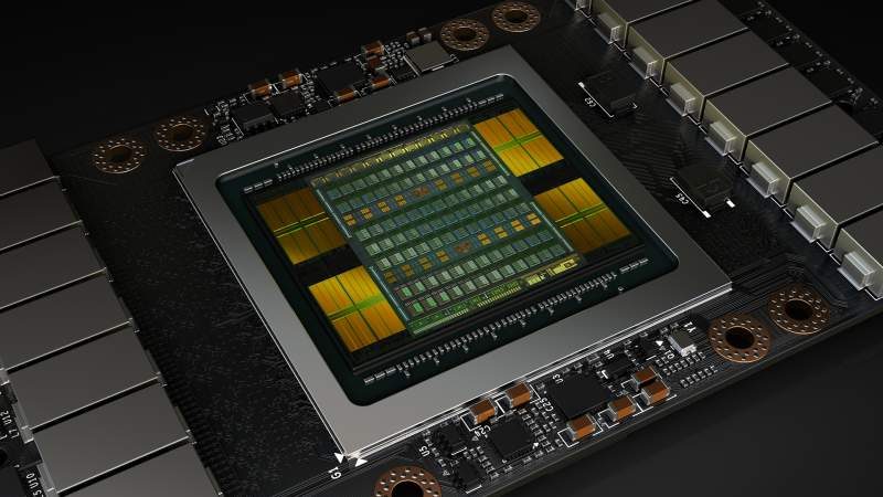
Most users familiar with graphics card are familiar with HBM2 (2nd Gen High-Bandwidth Memory) technology. It is used in NVIDIA‘s current top-end Volta GPU-powered products for example.
However, aside from high cost of implementation, it also faces capacity limitations in comparison to other memory technologies. Each stack is currently limited to 8GB, so the most a full card can have is 32GB. That is until the announcement of the latest JEDEC standard JESD235B.
What is New with the Addition of JEDEC JESD235B?
JESD235B bumps up to densities of up to 24 GB per stack at speeds up to 307 GB/s. This is across a 1024-bit wide device interface, feeding separately into 8 independent channels on each DRAM stack. The standard can support 2-high, 4-high, 8-high, and 12-high TSV stacks of DRAM at full bandwidth. This now allows system flexibility on capacity requirements from 1 GB to 24 GB per stack.
This update also extends the per pin bandwidth to 2.4 Gbps. It adds a new footprint option to accommodate the 16 Gb-layer and 12-high configurations for higher density components.

Now high-end video cards can have greater memory capacity using this high-bandwidth technology. The NVIDIA Tesla V100 HPC GPU for example can only fit a total up to 32GB (8GB x 4) HBM2. Now companies can fit a lot more without requiring additional space on the die. So you can expect up to 96GB HBM2 for such high-end GPUs in the near future.


