Nvidia Details Tesla P100 Pascal GPU Specifications
Samuel Wan / 9 years ago

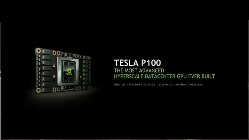
After revealing their next flagship Telsa earlier, Nvidia has let loose with a few more details and specifications. Based on the new Pascal architecture, the P100 will be utilizing TSMC’s latest 16nmFF+ process. As we know from the keynote, the chip will feature 15.3 billion transistors and the latest HBM2 memory. The P100 also features what Nvidia is calling the “5 miracles”.
First off, the P100 will run at an impressive 1328 MHz base clock and 1480 MHz boost. This is high for a professional Tesla card though well in line with GeForce clocks. The card won’t be using the full GP100 die with 60 SMs and 3840 CUDA cores, rather it will use a cut-down version with 56 SMs with 3584 cores. This mirrors Kepler’s launch where the cut-down Titan came before the Titan Black. In addition to the usual FP32 CUDA cores, there are also 1792 FP64 CUDA cores for Dual Precision Work. This gives a 2SP/1DP ratio, higher than anything from Kepler or Maxwell. The P100 also has 224 TMUs and massive amounts of cache and register files.

Next, we have the massive 610 mm² die on 16nmFF+. About 50% of that is FP32 CUDA cores, 25% is FP64 and rest on other parts. This means despite the massive die size, the P100 and GP100 derivatives won’t be great gamers, as games generally only use FP32 CUDA cores. There may be a GP100 variant though that swaps out the FP64 cores for FP32 ones. Even saddled with compute though, GP100 will still beat the Titan X by a good margin. TDP is a relatively tame 300W, as expected from the use of 16nm and 16GB of HBM2.
Finally, most marketing statements are hyperbole and the “5 miracles” are no exception. They are the Pascal Architecture, 16nm FinFET, CoWoS with HBM2, NVLink, and New AI Algorithms. Honestly, none of these are really that amazing on their own and have been expecting. Combining all of them in one go on such a massive chip though is pretty amazing though. While the P100 will be shipping soon, don’t expect many till Q1 2017.


