Nvidia Levels up with ‘Pascal’ Based Silicon in Works
Pratyush Shrivastava / 10 years ago

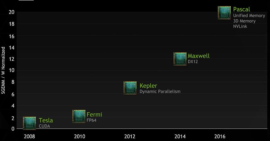
Nvidia has made a significant advancement in its product development cycle. Reportedly, it has managed to successfully figure out its next big silicon-based on its upcoming “Pascal” GPU architecture which is codenamed GP100. A successor to GM200, this chip will act as foundation to several others based on this architecture. The company has successfully fabricated a small quantity of working prototypes for internal testing and further development.
Nvidia, as expected, plans to follow its practices and release another chip targeted to gamer segment and is codenamed GP104 (successor to GM204). 3dcenter Speculates that the GP100 could sport anywhere between 4,500 to 6,000 CUDA cores. With this advancement, Nvidia will skip HBM1, which is making its debut with AMD’s “Fiji” silicon; and jump straight to HBM2, which will allow SKU designers to cram up to 32 GB of video memory. The chip will be built on TSMC’s upcoming 16 nanometer silicon fab process using either 16ff or improved 16ff+ process.
Specifications
- Architecture: Pascal “Stacked DRAM”
- Fabrication Process: 16nm production by TSMC (probably “16ff +”).
- DX Render: DirectX 12.1 hardware
- VRam: up to 32GB HBM2 memory.
Speculated
- 500-550mm² chip area
- 4500-6000 shader units
- 4096 bit DDR memory interface HBM2
It is speculated that GP 100 (professional segment) will be ready for release in Q2 / 2016 and GP 104 (gamers segment) in Q3 / 2016.
Thank you 3DCenter for providing us with this information.
Image courtesy of AnandTech.


