Rumour: Nvidia GTX 880 Pictured, 8GB and 375W TDP
Ryan Martin / 10 years ago
Over at the Chinese technology website MyDrivers they have managed to get pictures of an engineering sample of what is believed to be a GTX 880 graphics card. The card’s GPU has the marking 1421A1 which apparently means it was manufactured within the first 21 weeks of this year according to VideoCardz. The prototype card has 8GB of GDDR5 with 16 double-backed SKHynix H5GQ4H24MFR 0.5GB modules, the standard version might therefore have 4GB but 8GB models will probably be made available too.
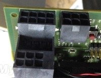
Despite the power efficiency of Maxwell, which we have seen with the GTX 750 Ti, this card comes with three PCIe power connectors: two 6 pins and one 8 pin meaning a maximum power draw of 375W. Of course it is unlikely a Maxwell card will need this much power since it is more efficient than Kepler and no single-GPU Kepler card required more than a 6 pin and 8 pin. The extra power connectors are probably for engineering sample testing purposes.
The main part of the graphics card aside from the GPU die area is hidden with pixellation: whatever is behind it is clearly important. Based on earlier rumours it might be ARM cores or there could just be unique identifiers in these parts of the board that might lead to the person who leaked these photos being reprimanded by Nvidia. The GPU die is rumoured to be GM210 by the source by other websites have suggested GM204 is more likely since this GPU die is larger than GK104 but smaller than GK110.
Source: MyDrivers
Images courtesy of MyDrivers


