SK Hynix’s High-Bandwidth-Memory Presentation Leaks
Bohs Hansen / 10 years ago
Our world of technology is going through some changes at the moment, some even call it a revolution. We’re finally starting to see some improvements in the display resolution that otherwise has been stuck for about 10 years, Internet-of-Things and wearable are the ‘new thing’ and the customers demands rise more with each advantage achieved.
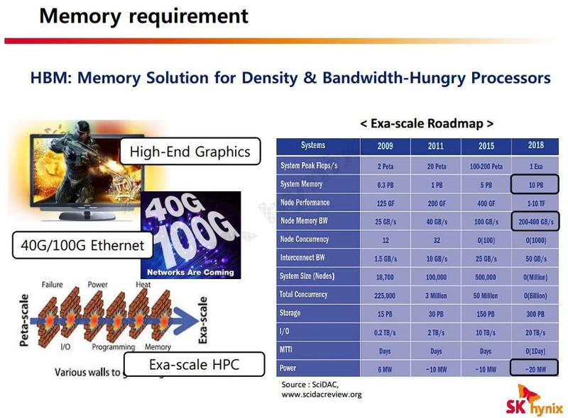
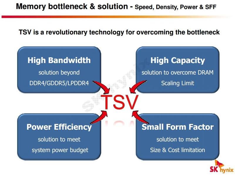
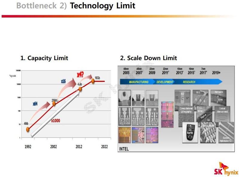
The memory is one of the things that really holds our progress back. We’ve reached a point where memory is the bottleneck in almost all situations, and we have to keep in mind that memory is everywhere. From LAN controllers to hard drives and not to mention your system or GPU memory. Memory and cache chips and dies are everywhere. There aren’t many electronics that don’t have some form of memory spread out across all their functions. And all of these can perform a lot better if the memory wasn’t throttling them. We will also need a lot more capacity, a lot smaller modules and a lot more power efficiency to carry out this revolution.
SK Hynix is working on that, and has been for a while. About nine month ago we learned that AMD had entered a cooperation with Hynix to work on the development of High-Bandwidth 3D Stacked Memory. A newly leaked slide show that originates back from August has found its way to Reddit in form of a PDF file. This new slide show gives us a lot more insight into all this and what it actually means.
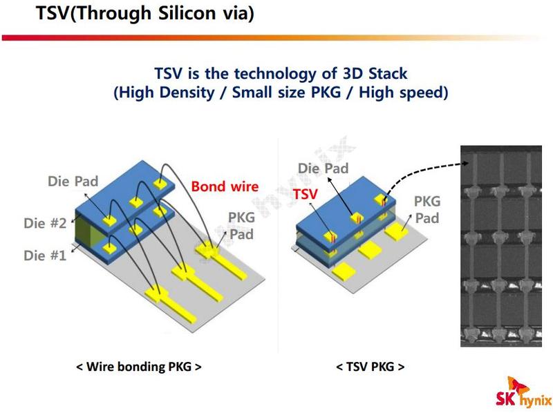
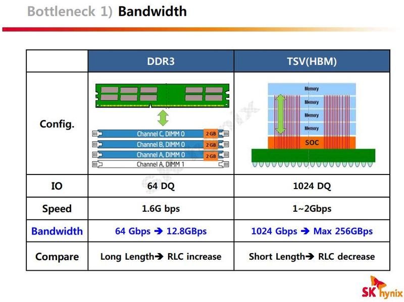
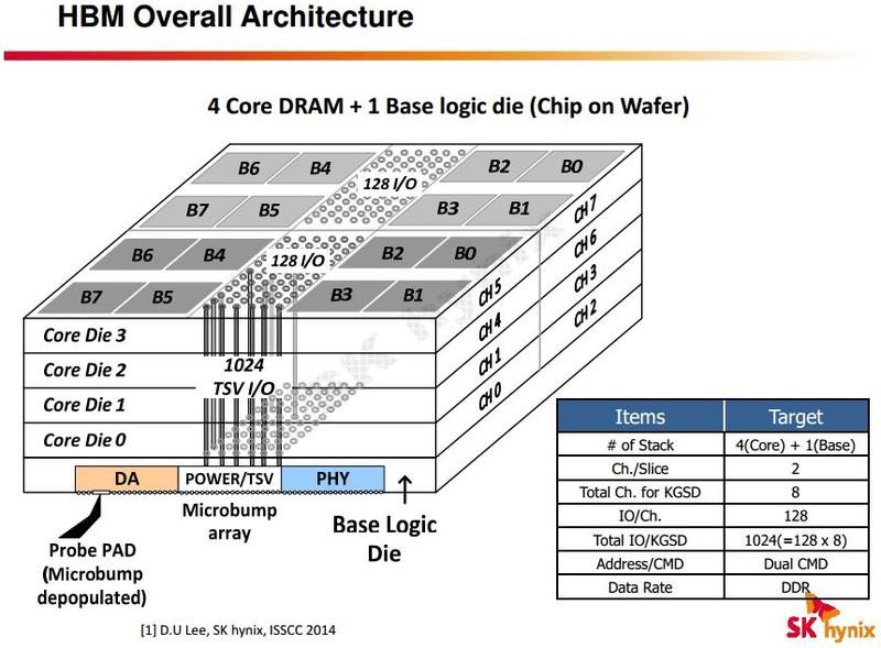
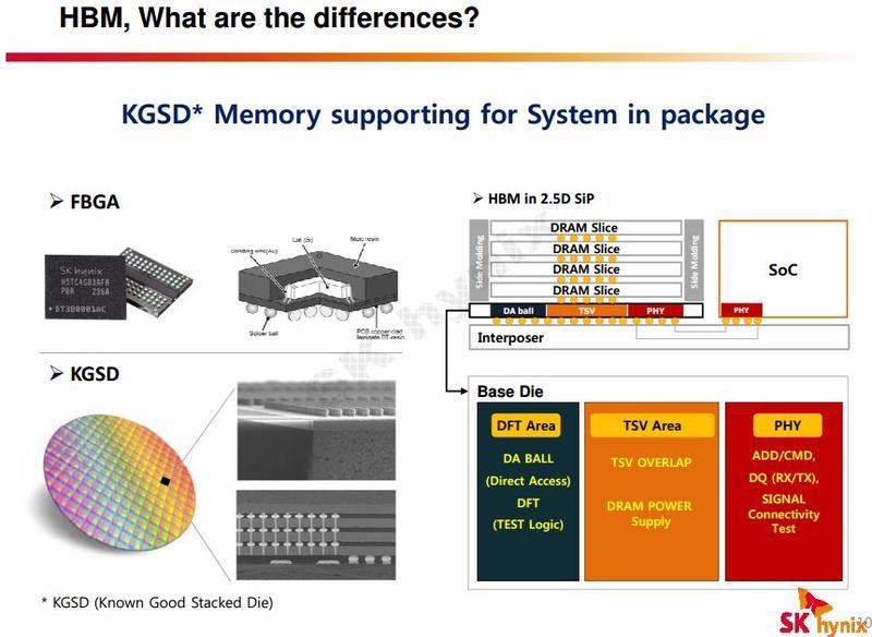
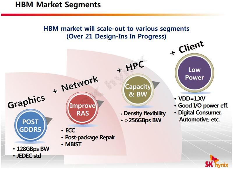
So what is High-Bandwidth-Memory (HBM) actually? It is a form of stacked DRAM designed to sit on top of each other. It seems a natural area for AMD to venture into and is something that could change the way their APU’s reside among the competition. There’s already a JEDEC standard defined for this as well. Oh, and did I mention that HBM will be capable of running up to nine times faster than the current GDDR5 memory?
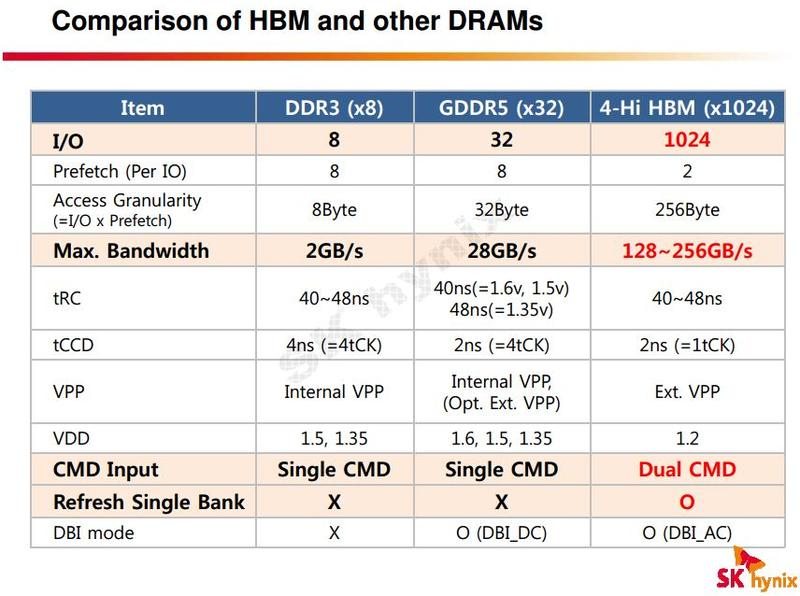
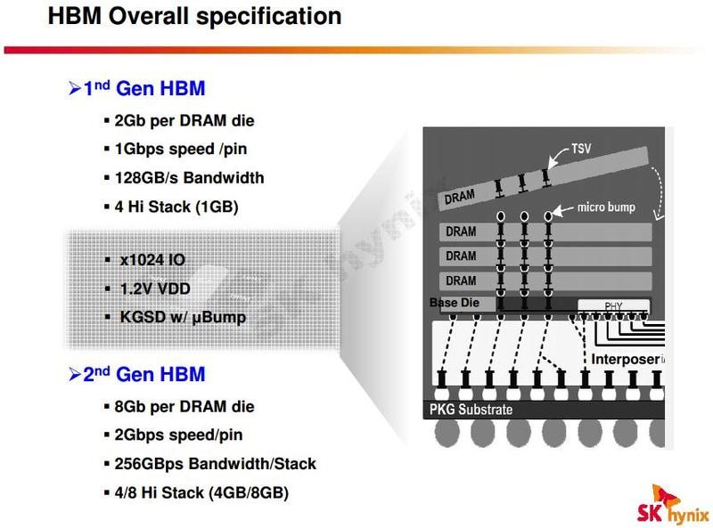
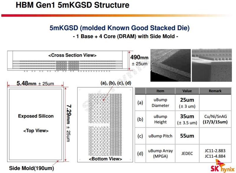
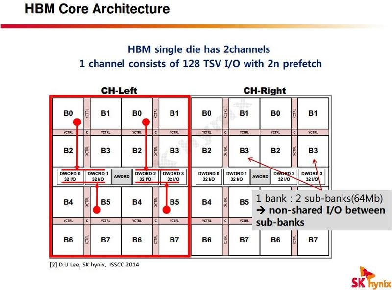
The first generation of the implementation will work with stacks of four DRAM dies on top of a single base layer where the dies are linked by vertical channels. They will provide 1 Gbps per pin and a total of 128 GB/s Bandwidth. The second generation will allow for up to 8 GB per DRAM die and double the speed to 2 Gbps per pin and 256 GB/s Bandwidth.
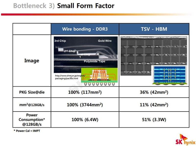
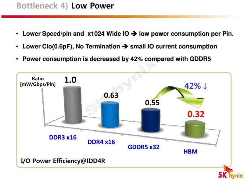
The presentation shows a roadmap that starts around new-year and goes all the way to the year 2023. The 128 GB/s is just the beginning and an indication of what lies ahead of us. It will be fast, it will be small and it will be power efficient, beyond what we know today.
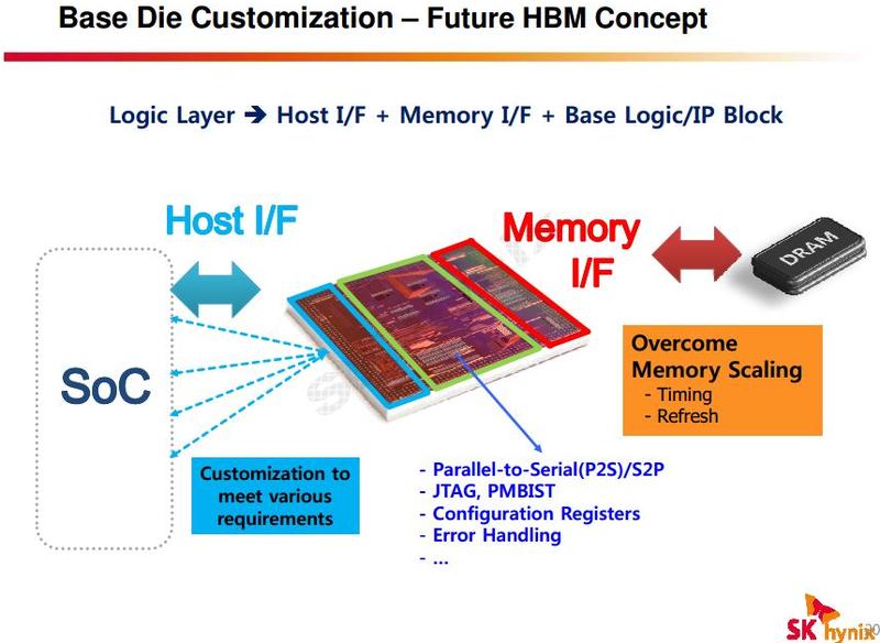
There are no actual products mentioned, but they are working 21 designs that all are in progress. One of those products could very well be the upcoming Carrizo APU that is rumoured to have stacked on-package memory. Another AMD product where this would fit extremely well is the next generation of AMD GPU’s. Do I dare say Radeon R9 380X / 390X? This is pure speculation from my side, but the time-frame adds up and it would be a logic move. It also fits with the leaks and rumours we’ve seen so far. I’m sure this is just the beginning.
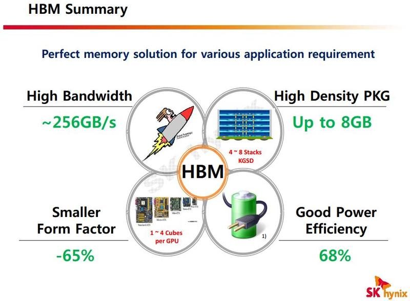
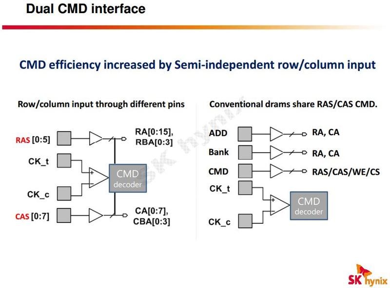
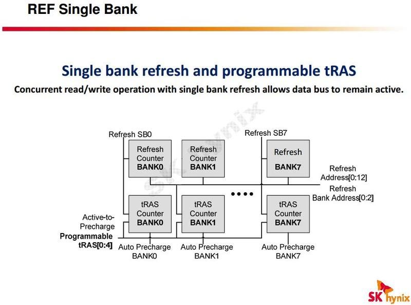
To sum it up a bit, the first generation of HBM is expected to deliver around 4.5 times the bandwidth of GDDR5. That’s 128 GB/s instead of 28 GB/s. At the same time we’re seeing a quadrupling on the capacity size while having a much smaller footprint. I’ll attach all the rest of the slides below the article, to let everyone create their own personal opinion on the leaked information.

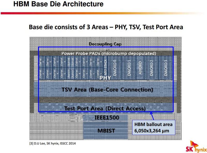
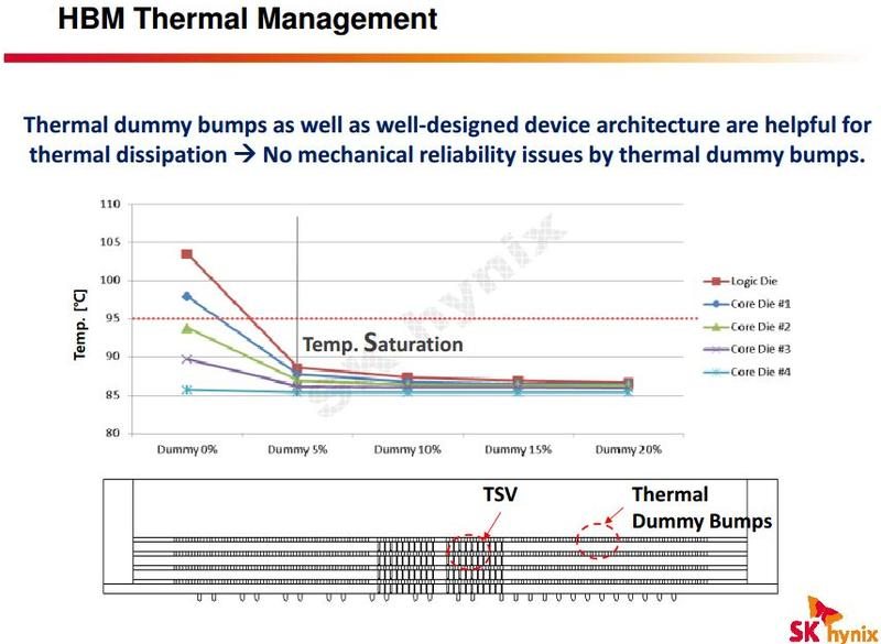
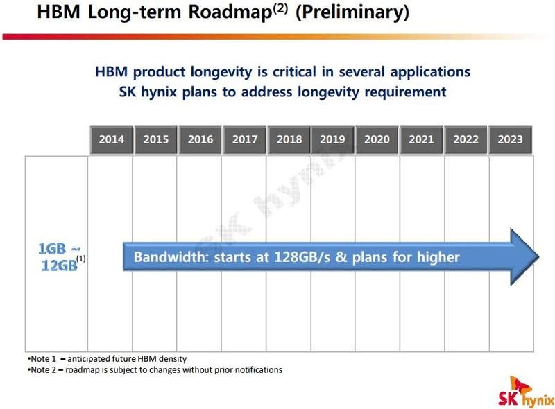
Thank you R_K_M on Reddit for supplying us with these information
